- 您现在的位置:买卖IC网 > Sheet目录3855 > PIC18LF1230-I/ML (Microchip Technology)IC PIC MCU FLASH 2KX16 28QFN
PIC18F1230/1330
2009 Microchip Technology Inc.
DS39758D-page 109
12.1
Timer0 Operation
Timer0 can operate as a timer or as a counter.
Timer mode is selected by clearing the T0CS bit. In
Timer mode, the Timer0 module will increment every
instruction cycle (without prescaler). If the TMR0
register is written, the increment is inhibited for the
following two instruction cycles. The user can work
around this by writing an adjusted value to the TMR0
register.
Counter mode is selected by setting the T0CS bit. In
Counter mode, Timer0 will increment, either on every
rising or falling edge of pin RA4/T0CKI/AN2/VREF+.
The incrementing edge is determined by the Timer0
Source Edge Select bit (T0SE). Clearing the T0SE bit
selects the rising edge.
When an external clock input is used for Timer0, it must
meet certain requirements. The requirements ensure
the external clock can be synchronized with the internal
phase clock (TOSC). Also, there is a delay in the actual
incrementing of Timer0 after synchronization.
12.2
Prescaler
An 8-bit counter is available as a prescaler for the Timer0
module. The prescaler is not readable or writable.
The PSA and T0PS2:T0PS0 bits determine the
prescaler assignment and prescale ratio.
Clearing bit PSA will assign the prescaler to the Timer0
module. When the prescaler is assigned to the Timer0
module, prescale values of 1:2, 1:4, ..., 1:256 are
selectable.
When assigned to the Timer0 module, all instructions writ-
ing to the TMR0 register (e.g., CLRF TMR0, MOVWF TMR0,
BSF TMR0, x
..., etc.) will clear the prescaler count.
12.2.1
SWITCHING PRESCALER
ASSIGNMENT
The prescaler assignment is fully under software
control (i.e., it can be changed “on-the-fly” during
program execution).
12.3
Timer0 Interrupt
The TMR0 interrupt is generated when the TMR0
register overflows from FFh to 00h in 8-bit mode, or
FFFFh to 0000h in 16-bit mode. This overflow sets the
TMR0IF bit. The interrupt can be masked by clearing
the TMR0IE bit. The TMR0IF bit must be cleared in
software by the Timer0 module Interrupt Service
Routine before re-enabling this interrupt. The TMR0
interrupt cannot awaken the processor from Sleep
mode, since the timer requires clock cycles even when
T0CS is set.
12.4
16-Bit Mode Timer Reads and
Writes
TMR0H is not the high byte of the timer/counter in
16-bit mode, but is actually a buffered version of the
high byte of Timer0 (refer to Figure 12-2). The high byte
of the Timer0 counter/timer is not directly readable nor
writable. TMR0H is updated with the contents of the
high byte of Timer0 during a read of TMR0L. This
provides the ability to read all 16 bits of Timer0 without
having to verify that the read of the high and low byte
were valid due to a rollover between successive reads
of the high and low byte.
A write to the high byte of Timer0 must also take place
through the TMR0H Buffer register. Timer0 high byte is
updated with the contents of TMR0H when a write
occurs to TMR0L. This allows all 16 bits of Timer0 to be
updated at once.
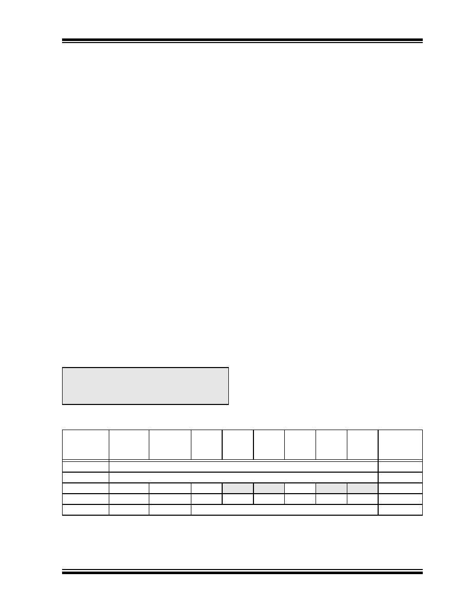
TABLE 12-1:
REGISTERS ASSOCIATED WITH TIMER0
Note:
Writing to TMR0, when the prescaler is
assigned to Timer0, will clear the
prescaler count but will not change the
prescaler assignment.
Name
Bit 7
Bit 6
Bit 5
Bit 4
Bit 3
Bit 2
Bit 1
Bit 0
Reset
Values on
Page:
TMR0L
Timer0 Register Low Byte
TMR0H
Timer0 Register High Byte
INTCON
GIE/GIEH
PEIE/GIEL TMR0IE
INT0IE
RBIE
TMR0IF
INT0IF
RBIF
T0CON
TMR0ON
T016BIT
T0CS
T0SE
PSA
T0PS2
T0PS1
T0PS0
TRISA
RA7(1)
RA6(1)
PORTA Data Direction Control Register
Legend:
— = unimplemented locations read as ‘0’. Shaded cells are not used by Timer0.
Note 1:
RA6 and RA7 are enabled as I/O pins depending on the oscillator mode selected in CONFIG1H.
发布紧急采购,3分钟左右您将得到回复。
相关PDF资料
PIC16LC711-04/SS
IC MCU OTP 1KX14 A/D 20SSOP
PIC18F65K22-I/MRRSL
MCU PIC 32K FLASH MEM XLP 64QFN
PIC16LF87-I/SS
IC MCU FLASH 4KX14 EEPROM 20SSOP
PIC16C62B-20/SS
IC MCU OTP 2KX14 PWM 28SSOP
PIC16LC711-04I/SO
IC MCU OTP 1KX14 A/D 18SOIC
PIC18F66J90-I/PT
IC PIC MCU FLASH 64KB 64-TQFP
ATMEGA32L-8AC
IC AVR MCU 32K LV 8MHZ COM44TQFP
DSPIC30F2012-30I/SP
IC DSPIC MCU/DSP 12K 28DIP
相关代理商/技术参数
PIC18LF1230-I/P
功能描述:8位微控制器 -MCU 4KB 256byt-RAM 16I/O RoHS:否 制造商:Silicon Labs 核心:8051 处理器系列:C8051F39x 数据总线宽度:8 bit 最大时钟频率:50 MHz 程序存储器大小:16 KB 数据 RAM 大小:1 KB 片上 ADC:Yes 工作电源电压:1.8 V to 3.6 V 工作温度范围:- 40 C to + 105 C 封装 / 箱体:QFN-20 安装风格:SMD/SMT
PIC18LF1230-I/SO
功能描述:8位微控制器 -MCU 4KB 256byt-RAM 16I/O RoHS:否 制造商:Silicon Labs 核心:8051 处理器系列:C8051F39x 数据总线宽度:8 bit 最大时钟频率:50 MHz 程序存储器大小:16 KB 数据 RAM 大小:1 KB 片上 ADC:Yes 工作电源电压:1.8 V to 3.6 V 工作温度范围:- 40 C to + 105 C 封装 / 箱体:QFN-20 安装风格:SMD/SMT
PIC18LF1230-I/SS
功能描述:8位微控制器 -MCU 4KBFlash 256byte-RAM 16 I/O 8-bit Family RoHS:否 制造商:Silicon Labs 核心:8051 处理器系列:C8051F39x 数据总线宽度:8 bit 最大时钟频率:50 MHz 程序存储器大小:16 KB 数据 RAM 大小:1 KB 片上 ADC:Yes 工作电源电压:1.8 V to 3.6 V 工作温度范围:- 40 C to + 105 C 封装 / 箱体:QFN-20 安装风格:SMD/SMT
PIC18LF1320-I/ML
功能描述:8位微控制器 -MCU 8KB 256 RAM 16I/O RoHS:否 制造商:Silicon Labs 核心:8051 处理器系列:C8051F39x 数据总线宽度:8 bit 最大时钟频率:50 MHz 程序存储器大小:16 KB 数据 RAM 大小:1 KB 片上 ADC:Yes 工作电源电压:1.8 V to 3.6 V 工作温度范围:- 40 C to + 105 C 封装 / 箱体:QFN-20 安装风格:SMD/SMT
PIC18LF1320-I/P
功能描述:8位微控制器 -MCU 8KB 256 RAM 16I/O RoHS:否 制造商:Silicon Labs 核心:8051 处理器系列:C8051F39x 数据总线宽度:8 bit 最大时钟频率:50 MHz 程序存储器大小:16 KB 数据 RAM 大小:1 KB 片上 ADC:Yes 工作电源电压:1.8 V to 3.6 V 工作温度范围:- 40 C to + 105 C 封装 / 箱体:QFN-20 安装风格:SMD/SMT
PIC18LF1320-I/SO
功能描述:8位微控制器 -MCU 8KB 256 RAM 16I/O RoHS:否 制造商:Silicon Labs 核心:8051 处理器系列:C8051F39x 数据总线宽度:8 bit 最大时钟频率:50 MHz 程序存储器大小:16 KB 数据 RAM 大小:1 KB 片上 ADC:Yes 工作电源电压:1.8 V to 3.6 V 工作温度范围:- 40 C to + 105 C 封装 / 箱体:QFN-20 安装风格:SMD/SMT
PIC18LF1320-I/SOG
功能描述:8位微控制器 -MCU 8kBF 256RM 16I/O Lead Free Package RoHS:否 制造商:Silicon Labs 核心:8051 处理器系列:C8051F39x 数据总线宽度:8 bit 最大时钟频率:50 MHz 程序存储器大小:16 KB 数据 RAM 大小:1 KB 片上 ADC:Yes 工作电源电压:1.8 V to 3.6 V 工作温度范围:- 40 C to + 105 C 封装 / 箱体:QFN-20 安装风格:SMD/SMT
PIC18LF1320-I/SS
功能描述:8位微控制器 -MCU 8KB 256 RAM 16I/O RoHS:否 制造商:Silicon Labs 核心:8051 处理器系列:C8051F39x 数据总线宽度:8 bit 最大时钟频率:50 MHz 程序存储器大小:16 KB 数据 RAM 大小:1 KB 片上 ADC:Yes 工作电源电压:1.8 V to 3.6 V 工作温度范围:- 40 C to + 105 C 封装 / 箱体:QFN-20 安装风格:SMD/SMT